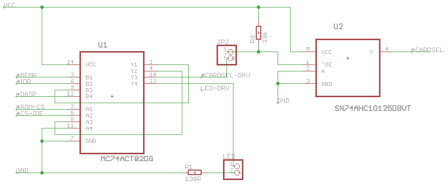
The 8237 DMA controller in the original PC/XT (and its clones) is fundamentally an 8-bit device with a 16-bit address space – perfectly matched to the MCS 85 family of which it was a part. So to make it work with the 20-bit address space of the 8086 and 8088, IBM added a 4-bit ‘page register’ for each of its four DMA channels using a 74LS670 (a quad 4-bit register file).
The 8237 and the 74LS670 though are broadly independent; the page register does not automatically increment when the address register wraps around to zero. This has two implications: normal segment:offset addresses must be converted to a linear, 20-bit physical address, and DMA transfers cannot cross a 64 KB page boundary.
Determining the Physical Buffer Address
Code in the XTIDE Universal BIOS illustrates how to convert a standard segment:offset address (presented in ES:SI) to a linear address, with just the 8088 instruction set:
     xor        dx, dx      ; clear DX
     mov        ax, es      ; copy ES to AX
 %rep 4
     shl        ax, 1       ; shift left 1, MSB into carry...
     rcl        dx, 1       ; ...and from carry to DX LSB
 %endrep                    ; repeat for the 4 MSB bits
                            ; AX now has ES SHL 4, and DX has ES SHR 12
     add        si, ax      ; add AX to SI, to get low 16-bits in SI
     adc        dl, dh      ; if it overflowed, increment DX (DH is zero)
     mov        es, dx      ; and save DX back in ES
DX needs to end up with ES SHR 12 because IBM hooked up the 74LS670 DMA page register to the low four-bits of the data bus, so programming the high 4-bits of the physical address is achieved from the low 4-bits of a CPU register. The addresses are then loaded into the DMA controller address register (in two halves, since the DMA controller has only an 8-bit data bus) and the associated page register. In this example, the port addresses are for channel 3:
     out        0Ch, al                ; Reset flip-flop to low byte
     mov        ax, es                 ; Get high 4 bits
     out        82h, al                ; Page register for Ch.3
     mov        ax, si                 ; Get low 16 bits
     out        06h, al                ; Send low byte to Ch.3 address register
     mov        al, ah                 ;
     out        06h, al                ; Send high byte to Ch.3 address register
Crossing a 64KB Boundary
Since the page register isn’t incremented by the DMA controller, a DMA transfer can run up to a page boundary at which point it (and the associated page register) must be re-programmed for another transfer into the next physical page. Splitting a transfer across a boundary therefore requires a check of the transfer size against the possible number of bytes up to a page boundary.
The code that follows assumes the maximum total transfer size is less than 64KB so allows for either one or two DMA transfers.
    ; On entry - buffer is in ES:DI, CX has bytes to transfer
    ; First calculate bytes up to physical page boundary
    mov        ax, di
    neg        ax                 ; 2s compliment

    ; if DI was zero, carry flag will be cleared (and set otherwise)
    ; When DI is zero only one transfer is required if total DMA
    ; transfer size is restricted to < 64KB
    jnc    .TransferDmaPageWithSizeInCX

    ; CF was set, so DI != 0 and we might need one or two transfers
    cmp        cx, ax                    ; if won't cross physical page boundary...
    jbe    .TransferDmaPageWithSizeInCX  ; ...perform transfer in one operation

    ; Calculate how much we can transfer on first and second rounds
    xchg        cx, ax            ; CX = BYTEs for first page
    sub         ax, cx            ; AX = BYTEs for second page
    push        ax                ; Save bytes for second transfer on stack

    ; Transfer first DMA page
    call    StartDMAtransfer
    pop         cx                ; Pop size for second DMA page

.TransferDmaPageWithSizeInCX:
    ; Fall to StartDMAtransfer

StartDMAtransfer:
    ; DMA controller programming and transfer is completed here
    ; This code will be hardware dependent
    ; ...

    ; Once transfer is done, update physical address in ES:DI
    ; since IO might need several calls through this function
    ; (if crossing a physical page boundary)
    mov        ax, es             ; copy physical page address to ax
    add        di, cx             ; add requested bytes to di
    adc        al, 0              ; increment physical page address, if required
    mov        es, ax             ; and save it back in es

    ret
Purpose
The DMA controller in the original IBM PC really has a few reasons for being – RAM refresh of course, background transfers (as used by SoundBlaster sampled audio for example), and high-performance transfers. The 8237 DMA controller is usually noted for its lack of performance, but that perception came about because CPU speed soon eclipsed it.
Operating in a 4.77MHz 8088, the DMA controller is the only way to transfer data to or from a peripheral in consecutive, back-to-back full-speed bus cycles (in later PCs, the DMA controller is throttled to about 5MHz to ensure peripheral compatibility). Of course it’s made more difficult by the boundary crossing issues and requirement to pause for RAM refresh, but the controller can provide the fastest possible transfers as demonstrated by my XT-CFv3 DMA Transfer Mode.


