When IBM released the PC/XT 5160, the 8 ISA slots were a welcome improvement from the 5 in the original IBM PC 5150; multi-function cards weren’t yet common and the system board itself provided no IO capabilities other than the speaker and keyboard, so everything needed an expansion card.
Whilst seven of the slots operated just like those in the 5150, the slot nearest the CPU was special – the IBM Technical Reference noting Slot J8 is slightly different from the others in that any card placed in it is expected to respond with a ‘card selected’ signal whenever the card is selected, the key being a previously unused signal line B8:
CARD SLCTD (I) Card Selected: This line is activated by cards in expansion slot J8. It signals the system board that the card has been selected and that appropriate drivers on the system board should be directed to either read from, or write to, expansion slot J8. Connectors J1 through J8 are tied together at this pin, but the system board does not use their signal. This line should be driven by an open collector device.
By observation, B8 needs to be asserted (low) only when reading from a device in slot 8, which then sets the direction of the buffer U15 to transfer data from the XD bus (housing slot J8, the system ROMs and the DMA controller) to the D bus (slots 1 to 7).
Open Collector Drive
For novices like me, the last part of IBM’s text is important: the open collector drive (see evilmadscientist.com for a good description of this). As other logic can drive B8, such as the ROM address decoder, a device driving ISA B8 can’t present a high-level drive when not asserted (the signal level is pulled up through RN1). This can be achieved either directly using open-collector logic, or by using a separate buffer.
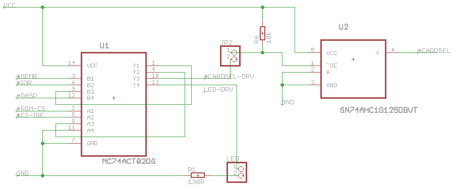
In my CPLD logic for the XT-CFv3, the logic looks like this:
In the Lo-tech CompactFlash Adapter, I’ve gone with a separate buffer by distilling the logic down to some NOR gates, to minimise component count (the NOR gate also providing LED drive):
There’s probably a better way, but both of those work anyhow 🙂
Zero Wait State
The CARD SLCTD use for B8 was pretty much limited to the IBM PC/XT 5160 – the later PC/AT re-purposed the line as a “zero wait state” line, which has particular advantage for 8-bit cards.
As IBM started pushing the processor clock rates up, ISA at the time being effectively a local bus, IBM chose to limit the effective bus speed for 8-bit cards by adding wait states to achieve a bus cycle time of about 750ns, roughly equivalent to the 4.77MHz speed of the original PC. At the time, expansion cards could be quite an investment so keeping things compatible was key.
Through the ZWS (B8) line in the PC/AT, and using the same basic logic as used to generate CARD SLCTD, the wait states can be eliminated for reads, and the logic simply extended to also consider IOW to also eliminate the wait states on writes. This can boost throughput by 30% on a 6MHz AT, and 50% on a later 12MHz AT class machine.


Trackbacks/Pingbacks