XT-CF-lite rev.2
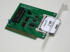
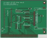
The lo-tech XT-CF-lite rev.2 is an 8-bit ISA CompactFlash adapter, providing bootable solid-state storage for any IBM compatible PC, including the original IBM Personal Computer 5150. The board supersedes the XT-CF-lite rev.1.
The CompactFlash card is accessible through a custom-made, 3D printed ISA expansion slot bracket, so it can be exchanged without opening the PC. The slot bracket includes CompactFlash specification guide rails for easy insertion and has a cutout to accommodate both Type I and Type II cards.
The board is based on SOIC 74xx series logic and utilises the 3M N7E50-Q516xx-50 CompactFlash socket, and has been tested with both CompactFlash cards and the Seagate ST1 microdrive.
The board is powered by the XT-IDE Universal BIOS, provided through an in-system re-programmable 32KB (addressible) flash-based ROM. Since the BIOS is only 8KB, 24KB is available for other purposes, and is byte-programmable.
This PCB is available now in the the TexElec Store.
Specifications
- Bootable 8-bit ISA Storage Adapter with header for single type I or type II CompactFlash or Microdrive media
- Provides fast, fixed-disk storage for 8-bit ISA slot equipped IBM compatible PCs
- Low power consumption and no external power connection required
- IBM Personal Computer XT System Board Slot 8 compatible
- Header for external device activity LED (12mA)
- Low-cost flash memory chip for boot ROM, 32KB usable (24KB available once boot ROM is installed)
- Configurable ROM base address - C800h or D800h
- Configurable IO Port base address - 300h or 320h (change require BIOS flash)
- Port-mapped IO; supports both 8- and 16-bit instructions (via partial address decoding)
- Utilises XT-IDE Universal BIOS (adapter type: 'XT-CF')
Design
Use of this design is provided subject to the lo-tech.co.uk Terms and Conditions. The design is Copyright (c) 2014 Peacon Ltd.
For general help with this kit, please see the XT-CF-lite FAQ.
Bill of Materials
| Part | Value | Package | Qty | Farnell | Mouser | Digikey |
|---|---|---|---|---|---|---|
| C1..6 | 0.1uF C-EUC0603 | C0603 | 6 | 1414610 | 963-UMK107BJ104KAHT | |
| C7 | 1uF C-EUC0805 | C0805 | 1 | 581-0805YD105K | ||
| C8 | 22uF CPOL-EUE2-5 | E2-5 | 1 | 647-UVR1C220MDD1TD | ||
| CF1 | N7E50-Q516xx-50 | N7E50-Q516xx-50 | 1 | 1267444 | 517-N7E50-Q516B-50-W | 3M5456CT-ND |
| JP1 | PINHD-2X04_2.54-S | 2X04-S | 1 | 571-5-146256-4 | ||
| IC1, IC2 | 74HCT688DW | SO20W | 2 | 1085321 | 771-74HCT688D-T | |
| IC3 | SN74LS33D | SOIC-14 | 1 | 1752958 | 595-SN74LS33D | |
| IC4 | 74ACT245DW | SO20W | 1 | 595-SN74ACT245DWR | ||
| IC5 | 74HCT139D | SOIC-16 | 1 | 595-SN74HCT139DR | ||
| IC6 | SST39SF0x0A | DIP32 | 1 | 1896595 | 804-39SF010A7CPHE | |
| R1 | 270R R-EU_R0603 | R0603 | 1 | 71-CRCW0603-270-E3 | ||
| RN1, RN2 | RESISTOR NETWORK, 10K, ± 2% | 1206 | 2 | 1770137 | 652-CAY16-103J4LF | |
| Socket | DIL32 | 1 | 1654375 | 517-4832-6000-CP |
- Board design permits the use of a range of DIP-32 flash chips or 1, 2 or 4Mb:
- SST39SF0x0A (SST39SF010A, SST39SF020A, SST39SF040A)
- AMIC A29010
- Regardless of the chip used, the first 32KB only will be mapped into the PC address space
- Base address configuration per JP1
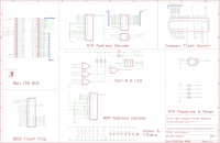
Logic
The board logic provides three distinct functions:
- ROM Function:
- IC2 matches the address bus to the selected base address
- JP1 position 3 being closed, the select signal is fed to the flash-ROM IC6
- CompactFlash interface via IC1, IC4 and IC5
- IC1 matches the address bus to the selected base address
- IC4 provides the data bus buffering, to ensure strong signal is driven onto the ISA bus
- IC5 provides CS0 and CS1 generation based on A4 (alternate status register is at Base+10h) and Reset signal
- Slot-8 Card Select Signal and activity LED drive are generated by IC3
- R1, RN2 and IC3 can be left unpopulated if slot-8 function and activity LED are not required
BIOS Flashing (Programming)
- The board is powered by the XT-IDE Universal BIOS and features a 32KB in-system re-programmable flash chip
- XTIDE Universal BIOS build R560 or newer is recommended (v2 beta 3 is much older)
- The flash chip is programmed with the Lo-tech XT-CF flash utility
- Select the appropriate ROM image:
- IDE_XT.BIN for Intel 8088 and 8086 CPUs
- IDE_XTP.BIN for NEC V20, V30, and Intel 80286 CPUs
Note: The late initialisation module in the XTIDE Universal BIOS should only be included in the BIOS build for systems that require this. The module can cause the BIOS to hang after initialisation on other systems. The BIOS build above excludes this module.
To program the board, make a DOS boot disk (utilities have been tested on MS-DOS 2.11, 3.3 and 6.22) and add the BIOS binary file and the flash utility. Install the Lo-tech ISA CompactFlash Adapter in the machine and boot from the floppy, then flash the ROM thus (assuming JP1 position 1 is closed, so setting the ROM base address to C800h):
A:\>flash ide_xt.bin c800
Note that should a board containing the IDE_XTP.BIN image be moved to an Intel 8088/8086 PC, the BIOS image will cause the machine to hang during the POST. To resolve this, either re-flash the board with the IDE_XT.BIN image before moving, or disable the ROM during the POST by opening JP1 position 3. JP1 position 3 can be closed once the machine has booted, so enabling the ROM for programming (provided there is no other ROM at the selected address).
ISA Bracket
Uses Lo-tech ISA Slot Bracket Type 2.
Board Configuration
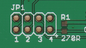
JP1 provides the ROM and IO port base address selection, ROM enable, and LED output.
| Position (per silkscreen) | Function | Open | Closed |
|---|---|---|---|
| 1 | ROM Base Address | D800h | C800h |
| 2 | IO Port Base Address | 320h | 300h |
| 3 | ROM Function | Disabled | Enabled |
| 4 | Activity LED | - | - |
Default settings are ROM enabled, IO port 300h and ROM base address C800h.
Note that the IO base address is set within the XTIDE Universal BIOS ROM image via the Universal BIOS Configuration and Flashing utility. The IO address set within that utility must match that configured on the card via the DIP switches. Should the IO port address be changed for any reason, the BIOS must be updated and re-flashed (using the lo-tech XT-CF flash utility).
Device activity LED output is provided at JP1 position 4. Do not short the output. Observe polarity ('+' side is noted on board silkscreen). The LED output is provided through a 270R resistor (R1), providing approx. 12mA.
