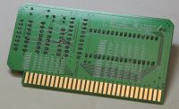
Lo-tech ISA ROM Board
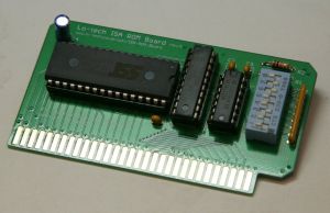
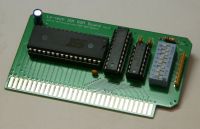
The Lo-tech ISA ROM Board (currently rev.3) is a simple and cheap to make 8-bit ISA board that provides a 32 or 64KB ROM via a flash chip, which can be (re)programmed a practically limitless number of times directly within the host PC via the lo-tech XT-CF flash utility. The board supersedes the Lo-tech 8-bit ROM Board.
This board can be purchased online via the TexElec Store.
Features
- Can be used to store any ROM image (or images) in any PC with an ISA slot
- In-system re-programmable via the lo-tech XT-CF flash utility
- DIP switches allow address base selectable between 8000h and F800h and configuration as either 32KB or 64KB
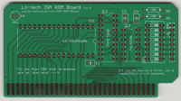
- DIP switch settings printed on board solder side
- Can be used in IBM Personal Computer XT System Board Slot 8.
- Uses only through-hole components, for simple home assembly.
To buy this and other PCBs, please visit the lo-tech shop.
PCB
The Lo-tech ISA ROM Board rev.3 PCB supersedes the Lo-tech 8-bit ROM Board, and has a revised BoM.
Use of this design is provided subject to the lo-tech.co.uk Terms and Conditions.
FAQ
How can I buy a PCB or kit?
Please visit the Lo-tech Shop
Do you offer ready-made boards?
The Lo-tech PCBs and kits are offered primarily as self-assembly kits.
Is there an assembly guide?
Please see Lo-tech PCB Assembly - General Notes.
How does it work?
The ISA bus consists of address signals ('address lines'), data lines, and read/write command lines. For each bus cycle, the address lines are set first, and the values held. Then on the next cycle, the read or write command signal is asserted, instructing the selected device to present or store data.
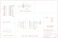
The values on the address lines are matched to the values set with the DIP switches by IC2, and when the values match the chip-select (ROM-CS) signal is asserted on the flash chip IC1. Next, the read or write command line is asserted, causing the flash chip to present or store data at the specified address.
The DIP switches provide a logic 1 or 0 (high or low) by being connected directly to 0V on one side, and to 5V on the other via 10K-Ohm "pull up" resistors. In the ON position, the connection to 0V 'wins' and a logic low (0V) is observed. In the OFF position, the only connection is to 5V via the resistors, so a logic high (5V) is observed.
To work in IBM Personal Computer XT System Board Slot 8, the card echos the read command back to the PC via a 'Card Select' line (ISA pin B8), which is done by a pair of NOR gates wired together in IC3. IC3 is an 'open collector' device, meaning it only drives the signal to a logic low (0V) - when ISA B8 is not driven by IC3, another device in the PC can drive it instead.
Bill of Materials
In addition to a blank PCB, these following parts are required to build a functioning board. When ordering a complete kit, everything in the table below, or equivalents, are included.
| Part | Device | Package | Qty | Farnell | Mouser |
|---|---|---|---|---|---|
| IC1 | SST39SF010A-70-4C-PHE | DIP-32 | 1 | 1896595 | 804-39SF010A7CPHE |
| IC2 | 74HCT688N | DIP-20 | 1 | 382504 | 771-74HCT688N |
| IC3 | 74LS33N | DIP-14 | 1 | 2076566 | - |
| R1, R2 | Carbon Film Resistor 10K | - | 2 | 9342419 | 279-CFR25J10K |
| RN1 | 10k Bussed Resistor Network | Bournes 4608X-101-103LF | 1 | 9356371 | 652-4608X-1LF-10K |
| C1..3 | 0.1uF Ceramic Capacitor | C025-030X050 | 3 | 2112751 | 581-SR205E104MAR |
| C4 | 10uF Electrolytic Capacitor | E2-5 | 1 | 8767084 | 647-UVR1C100MDD |
| Sw1 | MULTICOMP MCNDS-08-V | DIP16 | 1 | 9471596 | 774-2068ST |
| IC Socket (DIP32) | - | DIL32 | 1 | 1654375 | 571-1-390263-2 |
| IC Socket (DIP20) | - | DIL20 | 1 | 1101349 | 571-1-390261-6 |
| IC Socket (DIP14) | - | DIL14 | 1 | 1101346 | 571-1-390261-3 |
- Board design permits the use of a range of DIP-32 flash chips or 1, 2 or 4Mb:
- SST39SF0x0A (SST39SF010A, SST39SF020A, SST39SF040A)
- AMIC A29010
- Regardless of the chip used, the first 32KB or 64KB (only) will be mapped into the PC address space
- Base address configuration per DIP Switch Settings
DIP Switch Settings
Summary
| Switch | Function | On | Off |
|---|---|---|---|
| 1 | Slot-8 Function | Enabled | Disabled |
| 2 | ROM Enable | Enabled | Disabled |
| 3-8 | Address Selection (see below) | - | - |
- For 32KB operation, set 3 as required, 7 Off and 8 On
- For 64KB operation, set 3 On, 7 On and 8 Off
32KB Address Mapping
| Base Address | Sw3 | Sw4 | Sw5 | Sw6 | Sw7 | Sw8 |
|---|---|---|---|---|---|---|
| 8000h* | On | On | On | On | Off | On |
| 8800h* | Off | On | On | On | Off | On |
| 9000h* | On | Off | On | On | Off | On |
| 9800h* | Off | Off | On | On | Off | On |
| A000h | On | On | Off | On | Off | On |
| A800h | Off | On | Off | On | Off | On |
| B000h | On | Off | Off | On | Off | On |
| B800h | Off | Off | Off | On | Off | On |
| C000h | On | On | On | Off | Off | On |
| C800h | Off | On | On | Off | Off | On |
| D000h | On | Off | On | Off | Off | On |
| D800h | Off | Off | On | Off | Off | On |
| E000h | On | On | Off | Off | Off | On |
| E800h | Off | On | Off | Off | Off | On |
| F000h | On | Off | Off | Off | Off | On |
| F800h | Off | Off | Off | Off | Off | On |
* Note that these ranges aren't valid for option ROMs in PC architecture.
64KB Address Mapping
| Base Address | Sw3 | Sw4 | Sw5 | Sw6 | Sw7 | Sw8 |
|---|---|---|---|---|---|---|
| 8000h* | On | On | On | On | On | Off |
| 9000h* | On | Off | On | On | On | Off |
| A000h | On | On | Off | On | On | Off |
| B000h | On | Off | Off | On | On | Off |
| C000h | On | On | On | Off | On | Off |
| D000h | On | Off | On | Off | On | Off |
| E000h | On | On | Off | Off | On | Off |
| F000h | On | Off | Off | Off | On | Off |
* Note that these ranges aren't valid for option ROMs in PC architecture.
Sample ROM Image Files
8-bit IDE
A customised build of the XTIDE Universal BIOS (based on build r443) to enable CompactFlash media to be used connected to a standard 16-bit ISA IDE controller but installed in an 8-bit XT-class machine. The IDE controller must be using standard ports 1F0h and 3F0h.
Testing with with Diamond Flower MIO-400 KF REV F and Goldstar Prime 2 controllers, and expected to work with any standard IDE controller using the specified port addresses.
See http://code.google.com/p/xtideuniversalbios for official builds of the XTIDE Universal BIOS and source code.
Note, this is now an officially supported operating mode of the XTIDE Universal BIOS.
High-Density Floppy
XT compatible BIOS images to run high-density floppy drives, for example from 16-bit ISA multi-IO cards.
- FDC-BIOS.zip (courtesy of http://n8vem-sbc.pbworks.com)
- DTK-FDC-BIOS.zip (extracted from an 8-bit HD-FDC controller)
