Lo-tech XT-CFv2 Board
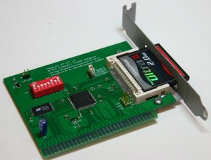
A development of the lo-tech XT-CF Board, the lo-tech XT-CFv2 Board has improved functionality and performance, and is slightly cheaper to make.
This board was superceded by the lo-tech XT-CFv3 Board, but ultimately these CPLD based cards were discontinued due to lack of CPLD availability. The below content is provided for reference only.
General Description
The lo-tech XT-CFv2 Board is a bootable 8-bit ISA to Compact Flash adapter for XT and AT class IBM compatible PCs. Like the original lo-tech XT-CF Board, the board offers a number of benefits:
- Replace dead MFM or RLL hard disks with a cheap compact-flash card or microdrive
- Easy to access compact-flash card (without opening the PC)
- Reduce system power consumption (and hence load on the PSU) by as much as 30W
- Uses the standard XT-IDE Universal BIOS (adapter type is 'lo-tech XT-CF')
- Increase system performance - offers 5x the throughput of an ST-412
- 32K in-system re-programmable ROM (with 24K free for any other ROM code)
In addition, the lo-tech XT-CFv2 Board also:
- Can be used in IBM Personal Computer XT System Board Slot 8
- Has reduced wait-state operation in PC/AT and newer hardware
- Provides the highest possible throughput in PC/XT class hardware via DMA mode operation
Developments from the lo-tech XT-CF Board
- Added CPLD connections to:
- ISA B8, to support PC/XT slot-8 and PC/AT zero-wait-state operation
- ISA DRQ3, DACK3, and TC, to support DMA transfers via channel 3
- ISA IORDY, to enable bus cycle extension should a CF card require it
- CF header IORDY, as above
- Reduced DIP switch to 8-way an eliminated switchable flash chip write enable line, due to software data-protection mechanisms included in the SST39SF series flash chips
- Changed 47uF capacitor (C1) hole spacing for cheaper 16V capacitors
Specifications
General
- 8-bit ISA card with header for type-I or type-II compact-flash media
- Compact-flash header configured to operate media in true-IDE mode
- 500mA 3.3V regulator can drive micro-drives or compact-flash cards without any external power connection (330mA power budget for micro-drives)
- Line driver for on-card and external activity LEDs (30mA power budget for external LED)
- Low-cost SMT Flash memory chip with 32K usable
- JTAG header for CPLD programming
Modes of Operation
- Port-mapped IO
- Memory-mapped IO
- DMA, via channel 3
Operating mode defaults to port-mapped IO, but can be switched on-the-fly between modes using the lo-tech XT-CF Configuration Utility.
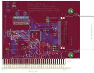
PCB
Boardhouse Requirements
- 8 mils clearances and minimum track width
- 0.4mm minimum hole size
- Can be manufactured on a 100x100mm board
- Gold fingers are preferable but not required
Prototyping is being undertaken using SeeedStudio Fusion PCB Service.
Assembly Notes
- Thoroughly wash the PCB before assembly with Isopropynol
- Place the CF socket, CPLD and flash chip first
- Next place the VRM, LED driver and resistor networks
- Then place LEDs, resistors and SMT capacitors
- Next thoroughly wash the board using a toothbrush to ensure flux is removed from between SMT pins
- Next add the through-hole components (DIP switch, headers and 47uF capacitor), then wash again
- Before use inspect all connections with a magnifying glass to ensure there are no shorts between pins. Inspect the CF header leads as solder can sometimes flow up the leads during assembly causing a short away from the PCB itself.
Programming the CPLD
See lo-tech XT-CF CPLD Programming Guide.
ROM & BIOS
ROM
- Board design permits the use of SST39SF0x0A flash chips (TSOP32, 8x14mm) of 1Mb, 2Mb or 4Mb capacity
- Regardless of the chip used, the first 32KB only will be mapped into the PC address space
- Base address configuration per DIP Switch Settings
BIOS
This card was supported by the XTIDE Universal BIOS.
Bill Of Materials
Farnell Parts List:
| Part(s) | Description | Package | Value | Qty Required | Farnell Code |
|---|---|---|---|---|---|
| IC1 | XC9572 72-cell 3.3v CPLD | TQFP100 | - | 1 | 1193233 |
| IC2 | SST39SF0x0A Flash | TSOP32 (8x14mm) | 1, 2 or 4Mb | 1 | 1829977 |
| IC3 | SCHMITT TRIG, INV GATE 74LVC1G14 | SOT-25 | - | 1 | 1893833 |
| VR1 | SPX3819M5-L-3-3 - LDO, 500MA, 3.3V, LOW NOISE | SOT-23-5 | - | 1 | 1831949 |
| C1 | Electrolytic Capacitor | Radial, 2mm pitch, 5mm diameter | 47uF to 100uF, 10V+ | 1 | 8767114 |
| C2, C14 | Ceramic Capacitor (X5R or X7R) | 0805 | 10uF, 10V+ | 2 | 1833812 |
| C12..13 | Ceramic Capacitor (X5R or X7R) | 0603 | 1uF, 10V+ | 2 | 1828801 |
| C3..11 | Ceramic Capacitor (X5R or X7R) | 0603 | 0.1uF, 10V+ | 9 | 1414610 |
| R2 | Resistor | 0603 | RESISTOR, 10K, 0.1W | 1 | 1469748 |
| R3, R5 | Resistor | 0603 | RESISTOR, 1K, 0.1W | 2 | 2008355 or 1652848 |
| R4 | Resistor | 0603 | RESISTOR, 270R, 0.1W | 1 | 2059585 |
| R6 | Resistor | 0603 | RESISTOR, 5K6, 0.1W | 1 | 1739171 |
| RN1, RN2 | Resistor Network | 1206 | RESISTOR NETWORK, 10K, ± 2% | 2 | 1770137 |
| LED1 | Low-current LED | 0805 | LED, SMD | 1 | 1685055 |
| SW1 | 8-way DIP switch | DIL | SWITCH, DIL, 8WAY | 1 | 9471596 |
| CF1 | 3M N7E50-Q516 Compact Flash Header | - | 3M N7E50-Q516xx-x0 | 1 | 1267444 |
| EXT.LED | 2-pin Header | - | HEADER, 1ROW, 2WAY | 1 | 3418285 |
| JP1 | 3-pin Header | - | HEADER, 1ROW, 3WAY | 1 | 3418297 |
| JTAG | 6-pin Header | - | HEADER, 2ROW, 6WAY | 1 | 3418492 |
| - | Jumper for CF Card Voltage Selection | - | - | 1 | 1740370 |
Notes:
- EXT.LED and R4 can be omited if external activity LED is not required
- LED and R5 can be omited if on-board activity LED is not required
- IC3, R4, R5, LED and EXT.LED can be omited if no activity LEDs are required
- There is no 'R1'
ISA Bracket
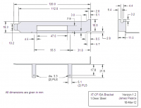
- ISA Bracket Design per sketch
- To minimise production cost, design has no threaded holes (simple nut-and-bolt required)
- Production likely to also exclude bending
- CAM Files: (in development)
Compatibility and Interoperability
Use with Other Cards
- The card can be configured to use DMA Ch.3 or not to - see DIP Switch Settings
- The IO port address set via the DIP switches must match that set in the XTIDE Universal BIOS configuration utility
- The BIOS address can be changed via the DIP switches without changing the BIOS itself
Media Compatibility
| Media | Type | Capacity | At 3.3V | At 5V | Tester |
|---|---|---|---|---|---|
| Extreme CF Adapter | SD to Type II CF Adapter | Dependent on SD Card | - | - | - |
| Kingston CF/128 | CF | 128MB | - | - | - |
| PQI Industrial | CF | 1 GB | - | - | - |
| SanDisk Ultra II | CF | 2 GB | - | - | - |
| SanDisk Ultra (30MB/s) | CF | 4 GB | - | - | - |
| Seagate ST1 | Microdrive | 5 GB | - | - | - |
| VERBATIM 44039 | CF | 4 GB | - | - | - |
Systems Compatibility
System compatibility has determined using the DOS Disk Tester utility with a pattern test of at least 10 passes of 4MB (the default).
| System | CPU | Status | Disk Tester Version | Tester |
|---|---|---|---|---|
| IBM PC 5150 | Intel 8088 | - | 2.3 | - |
| IBM Portable PC 5155 | Intel 8088 | - | 2.3 | - |
| IBM PC/XT 5160 | NEC V20 | - | 2.3 | - |
| Chaintech 5SIM | IDT WinChip P200 | - | 2.3 | - |
Performance
Factors Affecting Performance
- The host CPU speed
- The system type (PC/XT vs PC/AT)
- For PC/AT and newer systems, whether the BIOS can be shadowed in system RAM or not
- The operating mode (IO-mapped, memory-mapped or DMA)
- The multi-sector transfer support in the media
Many Compact Flash cards support only single-sector transfers, which results in increased BIOS overhead, particularly in DMA transfer mode (since the DMA controller must be programmed for each sector).
General Performance Notes
- IO-mapped transfer mode is slowest on all platforms but needs the least resources and has the best compatibility
- Memory-mapped transfer mode (enabled once DOS has booted with the lo-tech XT-CF Configuration Utility) offers increased performance but needs a 4KB transfer block available, for example at D800h.
- On PC/AT and newer systems, this (combined with ZWS configuration) will offer highest throughput
- This mode makes use of the bus interface logic by using 16-bit instructions (rep movsw), and therefore depends on proper implementation of that logic to work (some machines may not support this mode)
- DMA transfer mode (enabled once DOS has booted with the lo-tech XT-CF Configuration Utility) is fastest on PC/XT class hardware, but needs DMA Ch.3 available, so cannot be used if another device is using DMA Ch.3 (such as an MFM disk controller)
- ROM shadowing will offer significant performance gains on newer hardware, since the flash ROM is both 8-bit and ISA bus speed limited (BIOS code will be fetched much more efficiently from system RAM)
Sample System Measured Throughput
| System | CPU | Transfer Mode | Media type | Throughput |
|---|---|---|---|---|
| IBM PC/XT | 4.77MHz 8088 | IO-mapped | CF card supporting single-sector transfers | 150KB/s |
| IBM PC/XT | 4.77MHz 8088 | DMA | CF card supporting multi-sector transfers | 500KB/s |
| Amstrad PC2086 | 12.5MHz 80286 | Memory-mapped ZWS | CF card supporting multi-sector transfers | 1MB/s |
| Generic Pentium | 200MHz Pentium | Memory-mapped ZWS | CF card supporting multi-sector transfers | 1.6MB/s |
DIP Switch Settings
| Switch | Function | On | Off |
|---|---|---|---|
| 1 | IO Port A8 | 1 | 0 |
| 2 | IO Port A6 | 1 | 0 |
| 3 | ISA B8 / DMA Functions | ISA B8 Enabled | DMA Ch.3 Enabled |
| 4 | ISA B8 Function Type (if enabled) | PC-AT (Zero-wait-state) | PC-XT Slot 8 |
| 5 | ROM A17 | 1 | 0 |
| 6 | ROM A16 | 1 | 0 |
| 7 | ROM A15 | 1 | 0 |
| 8 | ROM Enable | Enabled | Disabled |
Default settings are:
- IO port 300h
- DMA Operation Enabled and ISA B8 function disabled
- ROM base address D000h
- ROM enabled
| 1 | 2 | 3 | 4 | 5 | 6 | 7 | 8 |
|---|---|---|---|---|---|---|---|
| ON | OFF | OFF | OFF | OFF | ON | OFF | ON |
IO Range
| IO Port Base Address | Sw1 | Sw2 |
|---|---|---|
| 200h | OFF | OFF |
| 240h | OFF | ON |
| 300h (Default) | ON | OFF |
| 340h | ON | ON |
Note that the IO base address is set within the XTIDE Universal BIOS ROM image via the Universal BIOS Configuration and Flashing utility. The IO address set within that utility must much that configured on the card via switches 1 and 2. Should the IO port address be changed for any reason, the BIOS must be updated and re-flashed to the XT-CFv2 card (using the lo-tech XT-CF flash utility).
ROM Base Address
| ROM Base Address | Sw5 | Sw6 | Sw7 |
|---|---|---|---|
| C000h | OFF | OFF | OFF |
| C800h | OFF | OFF | ON |
| D000h (Default) | OFF | ON | OFF |
| D800h | OFF | ON | ON |
| E000h | ON | OFF | OFF |
| E800h | ON | OFF | ON |
The BIOS address is determined at boot time by the XTIDE Universal BIOS. Since the code has been designed to be relocatable, the BIOS base address can be changed with switches 5-7 without the need to reconfigure the Universal BIOS.
Note that the BIOS base address is not related to the memory-mapped IO transfer address, except that the two ranges cannot overlap - see the lo-tech XT-CF Configuration Utility.
ISA B8 and DMA Function
ISA B8 in the PC/XT was used as a card select line to read from a card physically in the ISA slot closest to the CPU (known as slot 8), and has no function in other slots in the PC/XT. Preliminary research has shown that it's also unconnected in PC/XT clones (including, for example, the Tandy 1000TL despite that being an Intel 80286 based machine). In PC/AT and above, the line was used instead to shorten card access cycles by eliminating wait-states.
The logic design of the PC/XT system board prevents DMA transfers being performed from slot 8, so slot 8 function and DMA are mutually exclusive. Also note that memory-mapped transfers, that benefit from reduced wait states, are faster for PC/AT class hardware. Therefore, switch 3 switches between DMA or slot 8 / reduced wait states.
However, for the XT-CFv2 card to co-exist in a system with an MFM controller or other device that requires DMA Ch.3, DMA must be disabled by setting switch 3 to ON. The card doesn't though need to be in slot 8, since the line serves no purpose in the other slots.
Sample switch positions:
| Card Placement | DMA function | Sw3 | Sw4 |
|---|---|---|---|
| PC/XT or clone | Enabled | OFF | OFF |
| PC/XT or clone | Disabled | ON | OFF |
| PC/XT slot-8 | Disabled | ON | OFF |
| PC/AT or newer | Disabled | ON | ON |
Known Issues
- Activity LED is lit when a CF card isn't inserted. Could be resolved by adding a 50k PU to /PDIAG.


